@billy
Forum Replies Created
-
AuthorPosts
-
 BillyModerator
Post a picture of it Phil
Make sure you don’t have any solder bridges or strands of wire causing a short etc
BillyModeratorHard to tell but C3 looks the wrong way around on both builds
BillyModeratorLudo post some images of your build both sides of the pcb so that all the components and offboard wiring to DC jack in and out jacks and 3PDT switch can be clearly seen and traced
BillyModeratorThose resistors are feedback resistors a higher value will increase gain lower values will decrease it
The capacitors will be fine to use Elliott
It may not sound exactly like a triangle muff but it will definitely sound like a big muff
For more information have a look at the beginners guide to effects pedal components on the guides page
Here’s a guide to the big muff circuit from Kitrae
http://www.kitrae.net/music/big_muff_guts.html
BillyModeratorIn the emerald ring those are not actually clipping diodes they’re used as part of the rectification circuit
There’s a few mods discussed here
https://www.diystompboxes.com/smfforum/index.php?topic=119174.0
The tone tweq is an active tone circuit, to tighten up the low end you’re better experimenting with C4 and associated resistors, although I’d personally leave it alone because it boosts and cuts frequencies so you could get your desired tone in conjunction with the other pots ie cut treble boost bass etc
BillyModeratorIt sounds like something is mis biased
Post the voltages for all transistors and ICs
Q5 pins are C, B, E (collector, base, emitter)
https://www.componentsinfo.com/2n3906-transistor-pinout-details-equivalent/
Q1 to 4 pins are D, G, S (drain, gate, source)
https://www.componentsinfo.com/2n5457-transistor-pinout-equivalent/
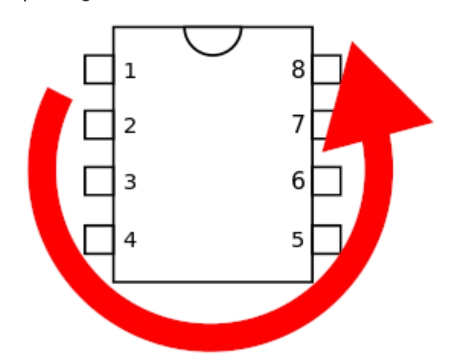
IC pins are numbered from the dot or notch pin 1 down and up and around in a U shape like this
The phasing sweet spot is around 2.2 to 2.5v on the FET gate pins set using the trimmer, all gate pins are connected as you can see in the schematic so you’d only need to set voltage on one then obviously check they all read the same
As far as I can see all your component values and orientation are correct
If you’re unsure how to check voltages using your meter set it to 20v DC place your black probe on a ground point and your red probe to each transistor and IC pin
BillyModeratorTry reducing the value of the gain pot
BillyModeratorPost pictures so that all component values and orientation can be clearly seen and offboard wiring traced
What voltages do you get on the IC pins
BillyModeratorLooks like you’ve got your trimmers mixed up TR1 is 100K (104) TR2 10K (103)
BillyModeratorBottom left corner of the pcb SW1 pads Earl
BillyModeratorI’d personally reflow any solder joints that look dull, grey, ball like or crumbly
It could be a few things causing the noise in the 2nd video, even something as simple as a dry solder joint especially on a capacitor or cross talk from audio wires running in paralell or too close to power wires a poor ground connection etc
Visually inspect your solder joints under magnification making sure there’s a good solder connection between component pin and solder pad
The FET is a unity gain amp / buffer the 5485 would be ok that’s not to say it wouldn’t cause it, especially if it’s fake where did you get it
You can also use the non technical method of touching or wiggling with a non conductive item like a plastic pen to see if it affects the noise or dab your finger on and off solder joints this may help narrow down your problem area
You obviously need to try and keep the pcb from moving whilst you do it
Make sure your transistor is fully in it’s socket
You can also touch the transistor with your finger to see if it affects it.
BillyModeratorWith Q1 out of socket your base voltage is correct and you wouldn’t get anything on the collector and emitter
Base voltage comes from the voltage divider R1 and 2
As you’ll know calculation is power in multiplied by resistor to ground R1 divided by R1 and R2 value in your case 8.7 x 100 / 570 = 1.52v
So you know that’s all good
Check your socket pins don’t have continuity and make sure you don’t have any microscopic bridges anywhere even a wisp of solder can cause problems
It appears that once you put your transistor in your problems begin it being an active device it may only cause a bridge when its connected in circuit, so it may not necessarily be a faulty transistor do you have a transistor tester
You are correct the tab does indicate the emitter and connects to R4 I wouldn’t think you’d damage the transistor if it was in the wrong way around it just wouldn’t conduct correctly
BillyModeratorI’d check R3 what voltages are you getting on Q1 pins check with it in and out of socket
Because you’ve got them socketed you could stick a jumper in Q1 base to collector to bypass the transistor obviously it won’t work as intended but it should let audio through and let you know if that’s your problem area
I’m taking it you’ve reflowed your socket joints
Everything that I can see looks to be the correct value and orientation those transistors don’t look like any I’ve seen in Barry’s shop what are they? They look like Motorola are they definitely PNP can’t find a datasheet
BillyModeratorUse your extra pole on the 3PDT for a bi colour LED use a common anode LED the type Barry sells
Get yourself a red /blue one then you could make blue and red correspond with the mod
Anyway like this, so common anode middle pin to 9v with a CLR (current limiting resistor) value will depend on how bright you want it, (remember though that the blue side will be dimmer than the red side regardless of CLR value)
Blue and red cathodes to the 2 outer lugs
https://drive.google.com/file/d/1EctV2-hH6ESs4SvWOPCpDwVXA3DPx1nd/view?usp=drivesdk
You’d want your red side cathode to be on the same side as the jumper and blue same side as your 47 to 100K resistor
If you’re unsure which side is which use a coin cell battery to light the LED
BillyModeratorLooking good Barry boy
Well done mate it’s definitely not easy breaking old habits
I can see a few gals chasing you soon so you better get in top shape and bolt like Usain….get outta there quick my man
BillyModeratorAre you connecting your in cable to the input jack remembering input is on the left wrong way up, that’s a fairly common mistake you’d still get bypass but no effect
There are a few solder joints that look like they lack solder and are potentially dry I’d reflow any solder joints that look dull, grey, ball like or crumbly especially on your 3PDT switch
Hold your iron tip on them for around 4 seconds until you see the solder pooling making sure you get a good connection between solder pad and component pin
Set your iron to 370°C
As far as I can see all values look correct
BillyModeratorDifficult to see
This is how it connects to the 3PDT yours obviously being modded on the in pad again its hard to see if your 3PDT lugs are horizontal like this
We’d need an image looking down on the 3PDT and pcb so that we can clearly see and trace the wiring
-
AuthorPosts