
Your Source for DIY Pedal PCBs and NostalgiTone! › GuitarPCB Forum › GuitarPCB Build Support › Space modulator bypass
Tagged: Space Modulator
- This topic has 16 replies, 3 voices, and was last updated 1 year ago by
 Billy.

-
AuthorPosts
-
September 5, 2025 at 6:23 pm #37287JasonWickershamParticipant
Alright everybody!
Spacemodulator build in the troubleshooting phase.
Issue: no bypass or efffected signal1: Have metered ground continuity through sleeve to sleeve, -ve DC jack, and DC jack -ve through sleeves.
2: Metered said ground continuity through all switches, and can demonstrate reeds are changing positions within switch body. Sleeve to Switch continuity appears proper.
3: Send/returns from each effect/3pdt header meter continuity
4: input to output pins on 3pdt breakout board meter good
5: LEDs all cycle properly
6: Tip continuity from jack tip to main I/O header (through jumper wires) meters good.
7: Tip to Tip, with all effect blocks bypassed NO CONTINUITY.
Im good about checking solder joints for overflow /shorts prior to soldering in pots, and also reflow after snipping excessive componet leads, and a visual inspection with good light and 10X loop indicated no overflow.
Any ideas?
Thank everybody in advance
PS: Barry, this batch of enclosures look AWESOME!! that powder blue is quite pleasant in person!
September 5, 2025 at 7:17 pm #37288BarryKeymasterWithout clear photos or voltage readings it’s a bit like trying to help a car that won’t start over the phone, we can definitely try, but we’ll need a few basics checked first:
-
Voltage regulators
-
Please confirm the exact part numbers (e.g., 78L05, L78L05, etc.).
-
Double-check Datasheet orientation: some regulators have reversed pinouts depending on package/brand. It’s surprisingly easy to install all three backwards if the silkscreen and part don’t match.
-
-
IC orientation
-
Verify every IC is seated the right way (notch/dot matches the board outline). There are a few in this build, so please check each one.
-
-
Trimmers
-
Set all three volume trimmers to 12 o’clock (Noon) as a starting point.
-
If that doesn’t get you there, the quickest way to locate the fault is an audio probe to trace the signal path and find exactly where it disappears.
Since the problem affects all three circuits, focus on parts common to all of them: the three voltage regulators (verify part numbers and orientation) and anything else that comes in threes—like the 3PDT footswitches. Make sure each switch is latching, not momentary. Each circuit contains a 4558 IC so make sure of orientation.
Alternatively, please provide voltage measurements for the ICs and regulators in an easy-to-read format so we can help diagnose remotely. For example:
-
Regulators
-
REG1 (part number): IN = _V, GND = _V, OUT = _V
-
REG2 (part number): IN = _V, GND = _V, OUT = _V
-
-
IC1 (part number):
-
Pin 1 = _V, Pin 2 = _V, … Pin 8 = _V
-
(and so on).
September 6, 2025 at 10:48 am #37294JasonWickershamParticipantSeptember 6, 2025 at 11:53 am #37295BarryKeymasterI wanted to make sure you got my message above regarding the minimum 100mA power supply requirement.
Your build can be perfect but nothing will work.
September 6, 2025 at 11:56 am #37296JasonWickershamParticipantOriginal testing yesterday was on a 9V 200mA iso output, and this morning on a 9V 1700mA supply.
September 6, 2025 at 12:23 pm #37297BarryKeymasterJust to confirm: you’re getting no signal at all—even with all three circuits in bypass—and when you test them one at a time (engage one, then return it to bypass before trying the next), there’s still no signal. Is that correct?
September 6, 2025 at 1:04 pm #37300JasonWickershamParticipantJust to confirm: you’re getting <strong data-start=”120″ data-end=”140″>no signal at all—even with all three circuits in <strong data-start=”173″ data-end=”183″ data-is-only-node=””>bypass—and when you test them <strong data-start=”207″ data-end=”224″>one at a time (engage one, then return it to bypass before trying the next), there’s still no signal. Is that correct?
Correct. I do hear a slight LFO bleed, but that is it. Think “lead plugged into amplifier without anything on the instrument side.” Switch state does not affect this at all.
Validated switches as well via meter. ringed out properly as a latching 3pdt should.
September 6, 2025 at 1:06 pm #37301BarryKeymasterUpdate: PT2399 at IC 2 looks good, however compare the IC 2 voltages with the voltages at IC5 PT2399 and you will see Pin 6 = 2.83V (too high). Also Pin 8 is too low at .69v
You can recheck if you think it was a measurement error.
As a fast test, swap the PT2399s; if the bad readings stay with the PCB position, it’s the surrounding parts, not the IC and vice versa.
The Reverb brick looks fine. This will take a while…
September 6, 2025 at 1:47 pm #37303JasonWickershamParticipantIC5, Pin 6: 2.48v , P8: 0.678v
Looks like I had a bad read on P6, but still seeing a low on P8. Swapping positions 2399, and will validate.
UPDATE: swapped em, plus attempted with a spare chip. Something going on with its neighbors
September 6, 2025 at 1:47 pm #37304JasonWickershamParticipantIC5, Pin 6: 2.48v , P8: 0.678v
Looks like I had a bad read on P6, but still seeing a low on P8. Swapping positions 2399, and will validate.
UPDATE: swapped em, plus attempted with a spare chip. Something going on with its neighbors
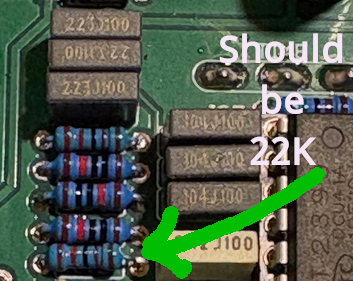
September 6, 2025 at 1:53 pm #37305BarryKeymasterYour R42 resistor should be a 22k which is Red – Red – Black – Red – Brown.
Looking at the image provided it does not appear to be that. Further that would absolutely skew the PT2399’s bias/RC network around pins 5–8 and would produce exactly the odd readings you saw (pin-6 too high ~Vref, pin-8 too low).
While the resistor in question above could technically be the Red stripes they do not match the brightness of Red of the surrounding resistors. You will have to decide.
September 6, 2025 at 1:53 pm #37307JasonWickershamParticipantR42 metered to 22K.
September 6, 2025 at 2:45 pm #37309BarryKeymasterI suggest a reflow with close attention to the socket pin soldering
PT2399 IC5 all pins and both ends of R39, R40, R41, R42. Inspect under magnification for:
• hairline bridge to ground near pin 8,
• lifted pin-8 pad,
• check for properly seated IC into the socket and good socket solder joints
• the small film caps (C31/C32 on that node) only to GND (no stray solder whisker touching a trace).To be clear the voltage discrepancy is not going to cause all three circuits to not work so that is something else.
Here is a generic checklist to follow
A) Prove each switch board in place (power off)
For each effect (#1 → #3), with the footswitch OFF (bypass):
-
IN → OUT (on that effect’s main-board header): should beep.
-
SND → RTN: should beep.
Expected continuity
Switch OFF (bypass):
-
IN ↔ OUT = beep
-
SND ↔ RTN = beep
-
IN ↔ SND = open
-
RTN ↔ OUT = open
Switch ON (engaged):
-
IN ↔ SND = beep
-
RTN ↔ OUT = beep
-
IN ↔ OUT = open
-
SND ↔ RTN = open
If any step fails, reflow the switch lugs on that board and the 6 ribbon pads on both ends for that effect. One bad joint here will kill all audio.
B) Verify order
Still power off—check that each net lands on the same labeled pad at both ends:
-
Main IN pad ↔ wiring-board IN pad = beep
-
Main SND ↔ wiring SND = beep
-
Main LED ↔ wiring LED = beep
-
Main GND ↔ wiring GND = beep
-
Main RTN ↔ wiring RTN = beep
-
Main OUT ↔ wiring OUT = beep
C) Walk the full bypass bus, jack-to-jack (all three OFF)
-
Input jack TIP → Effect #1 IN = beep
-
#1 OUT → #2 IN = beep
-
#2 OUT → #3 IN = beep
-
#3 OUT → Output jack TIP = beep
The first hop that doesn’t beep is the break (wire, header, or that 3PDT board).
September 6, 2025 at 3:30 pm #37315BarryKeymasterHere are some other quick check items:
With the pedal unpowered, TIP→TIP should still beep in full bypass. If it doesn’t, the fault is 100% in the bypass chain.
- Test inside the pedal first (unpowered, all bypassed).
If IN ↔ OUT beeps on the main-board pads, the pedal’s bypass path is good.
Now test the cables.
-
-
Plug one cable into IN, one into OUT; leave the far ends loose.
-
Meter tip→tip (free ends): must beep.
-
Meter sleeve→sleeve: must beep.
If either fails, it’s a bad cable or jack seating (scrape paint to bare metal around the jack holes).
-
-
Swap to two known-good TS instrument cables (no SilentPlug ends, etc) and retry.
Wiggle the plugs while metering—intermittents are common. -
If cables pass but there’s still no audio, re-check jack lugs with a plug inserted (tip of plug → wired TIP lug must beep). A wire on a switched or ring lug will kill pass-through just like a bad cable.
September 7, 2025 at 9:43 am #37318JasonWickershamParticipantSection C, part 4 on the ground walk. PM sent yesterday afternoon.
September 7, 2025 at 12:30 pm #37319BarryKeymasterTwo PMs were sent just now.
To summarize:
- RTN → TIP_OUT on the main PCB will read OPEN in bypass. That’s expected—the 3PDT only connects RTN <-> OUT when the effect is ON.
- The real pass-through check that should ALWAYS beep (regardless of ON/OFF) is the final hop from the last effect’s OUT₃ pad → TIP_OUT pad → output jack tip.
TEST (power OFF):
OUT₃ → TIP_OUT (main PCB pads) = beep
-
- If open: reflow both pads; if still open, add a tiny fly-wire OUT₃ → TIP_OUT on the PCB.
Jack TIP lug → actual tip of the inserted plug = beep
-
- If open: jack/plug seating or cable issue.
Bottom line: “RTN → TIP_OUT = no beep” in bypass is normal; failure on section C-4 (#3 OUT → Output jack TIP) points squarely to the final hop. Fixing OUT₃ <-> TIP_OUT <-> jack TIP will restore bypass and let the whole chain pass audio.
September 7, 2025 at 1:24 pm #37322BillyModeratorWhat I’d suggest you do is build a simple audio probe to check signal is actually getting into the circuit
With no effect or bypass signal it sounds like it could be something as simple as a poor connection or solder joint stopping audio either getting in or between each circuit or a faulty switch or jack etc
All you need is a mono jack a couple of bits of wire a 100n to 1u film or ceramic cap and a small croc clip or something to connect to ground see below image
Connect one leg of your capacitor to the tip lug with a wire to the other cap leg and something robust like a discarded diode or electrolytic cap pin to the wire end for your probe connect your other wire to the jack ground lug with a clip on the wire end to connect to a ground point
Ignore the first few building a probe pages in this PDF and read from page 6 using your probe
https://drive.google.com/file/d/1T9OsJ0riQhm1QFWPfNQ5q5guikuFKDRN/view?usp=drivesdk
The 3 circuits are connected in series like this so your signal would go from in jack to in on the first circuit switched to effects mode middle common row connected to top row it goes from in to snd1 into and through the circuit to rtn1 and so on
Middle common row connected to bottom row as you can see it goes along the trace to out bypassing the circuit and to in of the 2nd circuit
-
-
AuthorPosts




- You must be logged in to reply to this topic.