Your Source for DIY Pedal PCBs and NostalgiTone! › GuitarPCB Forum › GuitarPCB Build Support › ColorTone Supa TB v2 troubleshooting
- This topic has 22 replies, 6 voices, and was last updated 4 years ago by
 Anonymous.
-
AuthorPosts
-
May 5, 2022 at 7:28 am #24416AnonymousInactive
Hi everyone,
im building a ColorTone Supa TB v2 that I bought from Musikding. Before all the details, I’m having no Fuzz but everything else seems fine. There is a popping sound whenever I switch from bypass to effect and vice versa pointing in the direction of a grounding problem (maybe?). I had very low signal when the ground cables from the input/output jacks went straight to the board, as suggested in the manual. But all the build pictures I found those cables went to the 3pdt board. So I changed that. Now there is no signal at all when not in bypass. Is there a sheet with voltage values somewhere to begin troubleshooting further?
any further ideas are welcome.
greets, R
May 5, 2022 at 9:37 am #24418AnonymousGuestThere should not be any difference between the jack sleeves being connected to the main of the 3PDT board.
As you have made the connection to the 3PDT board, what then is still soldered to the GND of the in/out in the main board?
May 5, 2022 at 12:40 pm #24421AnonymousInactiveNothing. I pinched the cable off at the back. 🙂
May 5, 2022 at 6:34 pm #24424BarryKeymasterYou are going to have to show us how you wired it somehow.
There seems to be a wiring issue somewhere.
Many more pictures or draw it out.
You can also confirm your connections using a DMM.
This chart is old but still useful for troubleshooting.
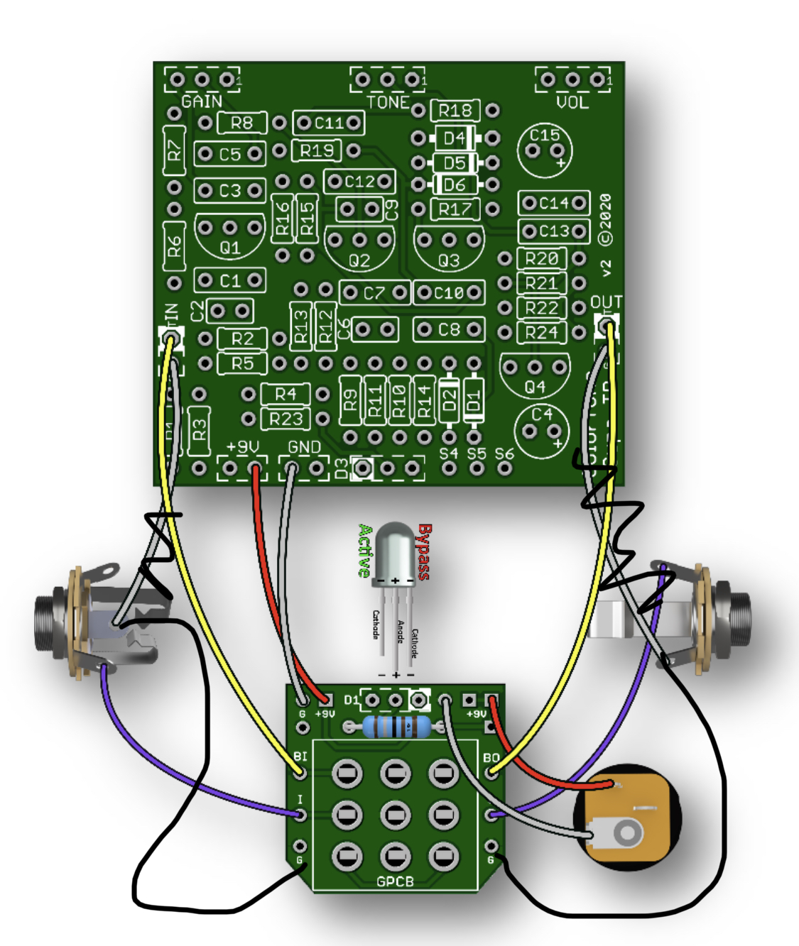
May 6, 2022 at 2:54 am #24429AnonymousInactiveThx for the reply. I used the following diagram. Then made the change that I drew in.
i tripple checked on different days. This is how I wired it up.greets
L
May 6, 2022 at 4:31 am #24430BarryKeymasterEither way would work.
Some of the wiring is actually backup and not mandatory but backup is better.
Be 100% sure that your PURPLE IN wire (photo above) from 3PDT (I) to Stereo Jack is going to actual TIP. Not all jacks are the same so do not just go by the drawing of the Jack and make sure it is TIP by connection and inspection.
Speaking of did you test your connections in Continuity mode using your DMM and the chart above?
May 6, 2022 at 8:54 am #24432AnonymousInactiveI checked it all with my DMM. I don’t find a problem other than no signal when engaged and the pop sound when switching. Bypass signal is flawless
May 6, 2022 at 10:06 am #24434AnonymousGuestOne more idea: the casing is on GND through sleeve contact of the Jack’s. Is there a possibility of contact of any other signal carrying part with the casing?
May 6, 2022 at 10:11 am #24435AnonymousGuestThe potentiometers may then cause a short circuit in case the cabling is interchanged.
May 6, 2022 at 10:43 am #24436AnonymousInactiveI looked for continuity between case and any of the pot connectors. All negative. Good idea.
May 6, 2022 at 11:52 am #24437Big OParticipantI have started making wiring diagrams for most of my recent pedal builds since jack locations can differ from pedal to pedal depending upon the drill template used for the particular enclosure. Plus some of the input jacks I have are different configurations. Making the diagram helps to prevent mistakes. Due to the tight constraints caused by the top mounted jacks and location of the LED of my Supa build, I had a grounding issue with the input jack (one of the lugs was touching the back of the pot). After I diagnosed it, I fixed the problem by rotating the input jack slightly and the pedal worked fine. Lately, I have resorted to testing each component before soldering it to the board as well as continuity testing as the build progresses. This makes it for slow building but much less of a chance of a problem once built. Below is my wiring diagram for the Supa with top mounted jacks.
May 6, 2022 at 1:03 pm #24439AnonymousInactive<hr />
I cannot find an issue with my wiring. 🙁 it must be the board
May 6, 2022 at 6:15 pm #24440CybercowParticipantPhotos of the solder-side of the PCB?
May 6, 2022 at 7:06 pm #24441BarryKeymaster+1 – I cannot see enough of what I need to see with just the photo above. It begs me to reach in the photo and start mauling over the entire board and while I am at it I would be re-flowing all solder joints and off-board wiring.
While it is technically possible, the chance of the board being faulty is extremely low.
So if after re-flowing (troubleshooting must do) we will need more good pictures and post some voltages as well.
Voltage right at the power jack first.
Then all of the transistors.
May 6, 2022 at 7:50 pm #24442AnonymousGuestI would also like to see good pictures of all off board wiring of pots and jacks.
BTW, the popping sound when switching from bypass to active can sometimes be caused by the foot switch itself.
May 8, 2022 at 3:31 am #24476AnonymousInactiveOk, let’s start with some Voltages:
@+9V: 9,45V
left to right
@Q1: 1,2V 1,6V 9,19V@Q2: 0,049V 0,66V 4,5V
@Q3: 9,3V 9,24V 9,4V
@Q4: 9,3V 9,2V 9,4V
q3 and q4 seem odd :/
picture of back of board:
popping sound also occurred when switching with my boss es-8 patch bay with effect on active.
May 8, 2022 at 3:54 am #24477AnonymousInactiveI measured continuity on the board a bit and discovered that there are some ground islands. For example R03, R07 and R014 all go to completely separated grounds. No continuity between them and only R03 goes to chassis ground. That’s not what I expected from the wiring diagram.
-
AuthorPosts


- You must be logged in to reply to this topic.