Your Source for DIY Pedal PCBs and NostalgiTone! › GuitarPCB Forum › General DIY Pedal Discussion › Desperately need help with Tayda kit
- This topic has 12 replies, 3 voices, and was last updated 1 week, 6 days ago by
 MixGtrz.
-
AuthorPosts
-
January 3, 2026 at 7:41 pm #38159MixGtrzParticipant
Hey all.
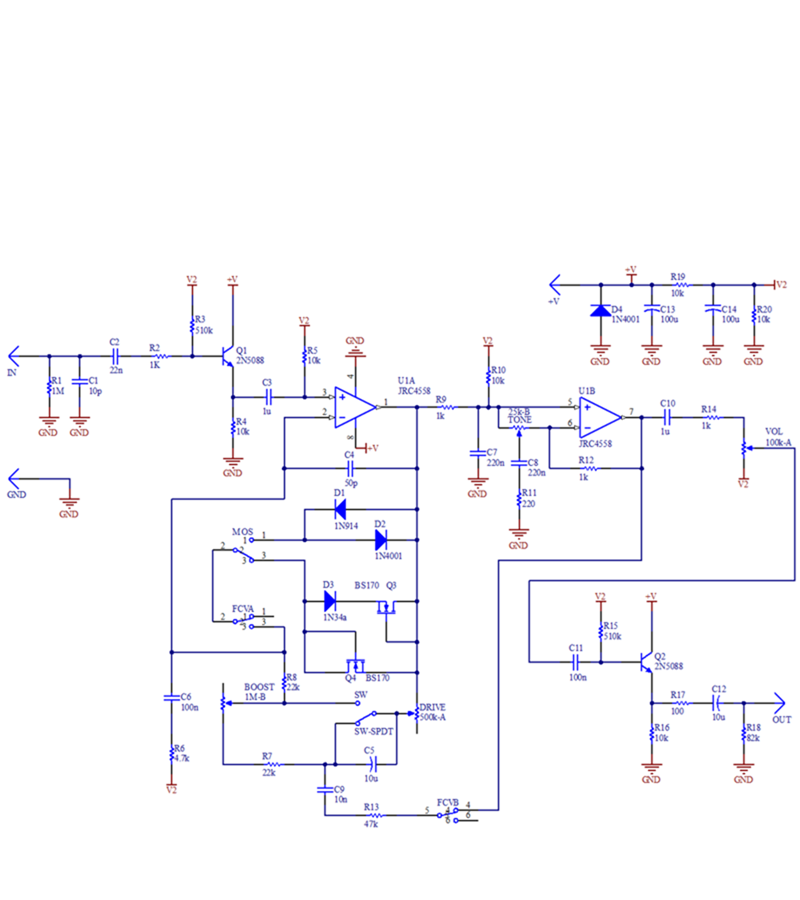
I built a Full Drive kit from Tayda but I’m having trouble with the switching circuit.
It uses a separate pcb for the dual footswitches (on/off & boost). Unfortunately there seems to be a problem with the switch pcb.
There is bypass signal, but the on/off switch does nothing and when the boost switch is engaged, it mutes.
I’m sure it is the switching that’s the problem as I was able to bypass the switches and the effect pcb is working.What I want to do is wire the switches without the pcb but I’m really struggling to figure that out. I’ve looked at lots of dual switch circuits and even a Fulltone schematic, but I’m sure none apply to this exact layout. I would assume the wiring configuration would need to reflect the the same path(s) as the pcb but I’m having difficulty sussing it out.
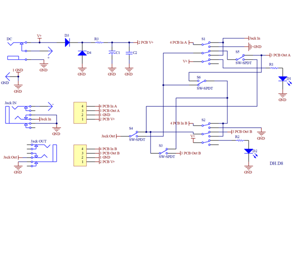
I’ve posted the two schematics in hope someone here can decipher them, and show me a diagram that 6th grader could understand. I know it’s a big ask, but any help would be greatly appreciated. I’m willing to pay for someone’s time.
NOTE: The switch circuit has noise filtering and polarity protection, but it’s not needed as the main pcb has it already. If you need more information, please just ask.TIA,
MickJanuary 3, 2026 at 8:27 pm #38161MixGtrzParticipantThe switch schematic doesn’t appear to have uploaded, so have reposted. Thanks!
January 4, 2026 at 5:39 pm #38165PlaysforfunModeratorAs long as V2 is created on the main pcb (R19 & R20), and the switches for MOS, SW and FCV physically connect to the main pcb then your circuit is complete and all you need a 3PDT board for effect on or bypass. You don’t mention pcb3 or pcb4 so i don’t know what the fancy switching is for.
January 4, 2026 at 6:35 pm #38167MixGtrzParticipantThanks Playsforfun.
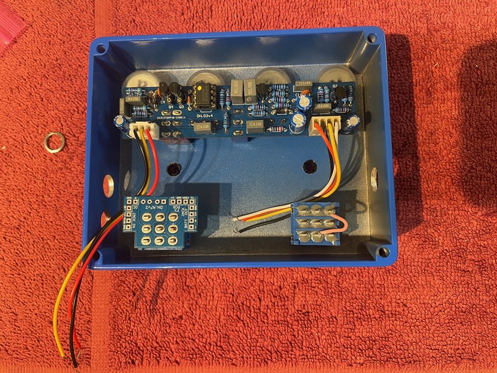
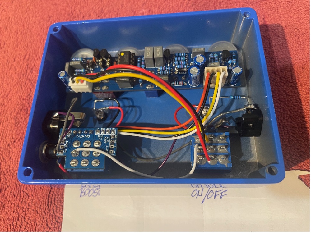
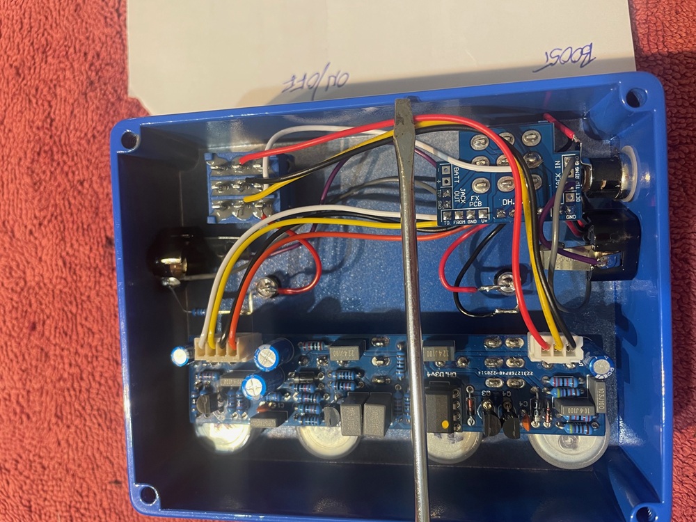
I’ve attached a photo of what I’m working with. I have two 3PDT pcbs, but assumed I only need the one (shown on Boost).
The 4 wires coming off the main pcb would presumably go the corresponding points on the switch pcb (V+, Gnd, From, To) (labels on main pcb on other side) but I’m at a loss as to how the two switches are connected together (particularly power for on/off LED an output jack).
I *think* the 3 wire connector goes to the three common lugs of the on/off switch. From top down (lugs), would go Red (4), Yellow (5), Black (6) and a jumper from 7to 6.From there, I haven’t a clue. And may be completely wrong on the above.
January 4, 2026 at 9:40 pm #38169PlaysforfunModeratorOk I checked this out at Tayda. The three wire connection is the boost on/off switch which is a footswitch in your case. The 4 wire connection is labeled on the board, as you said, and goes to the corresponding pad on the FS board. I can’t see where the current limiting resistor is mounted on that FS board but do not forget to use one between 2.2K and 4.7K. The other pads will wire according to their labels for in out and power and ground. Just a note that the power is input at this board and then wired to the main pcb. The footswitches should probably trade sides of the enclosure so that the 4 wires can reach the FS board. I see no reason for a 6 to 7 jumper as the boost switch will use a single column of the switch as a simple yes/no. Choose 1,2,3 or whichever. The second schematic that you attached is for a board you are not using that Tayda offers. Disregard it. A little ingenuity could factor in a led for that boost action if you wanted. Possibly what the 6,7 jumper is about. I’m not used to their methods. I’m all about Barry’s boards and methods.
January 4, 2026 at 11:07 pm #38170MixGtrzParticipantThanks again mate. That’s very helpful. I’ll wire it up as described and see how it goes.
re: power for the boost LED, there is a trace on the dual FS board that runs across from lug 2 of the boost switch to lug 2 of the on/off switch. When I apply power to the board, I get 9v at those lugs so I’ll try that after I get the FS’s functioning.
Also the FS board has the CLR on the switch side of the board. It’s kind of weird as the resistor is kind of stood up on one end!
I truly appreciate your help.January 8, 2026 at 7:25 pm #38189MixGtrzParticipantWell, still no joy…
I tried the suggestions that playsforfun offered, but it’s not working. However a slightly different result than the first one.
The on/off switch still does nothing (LED comes on). Just bypasses the signal. However with the Boost switch on, the master volume, tone and overdrive work (as you’d expect) but the boost level pot does nothing.I’ve tried changing the order of the 3 wires going to the on/off switch, as well as moving to lugs 7 8 9, and no change in function.
I think understanding the dual footswitch pcb scheme is critical here (which I don’t!). I’ve tried following the traces to map it out but get lost trying to relate it to the fx pcb.This has a lesson in just how much I don’t know…
January 9, 2026 at 9:30 am #38195PlaysforfunModeratorHow about some new pictures of the latest work. Maybe that could help.
January 9, 2026 at 12:35 pm #38198brdParticipantI might be able to simplify if further. your boost is switched on and off by making a connection between either the yellow and red or yellow and black wires from the 3 pin connector. you can try to manually connect them to verify the boost is switching on and off and working as expected. If that’s good, then wire the stomp switch accordingly. yellow on a middle pole and red and black on the corresponding throws. use an ohm meter to verify you have it oriented correctly.
January 12, 2026 at 12:54 am #38204MixGtrzParticipantHi All.
Sorry for the delayed response. Had other priorities unfortunately.
Anyway…
re: playsforun, I’ve post two new pics of the wiring per your suggestions.
re: brd, I know the boost section is working but have tried every possible order of the 3 wires on the common lugs of the on/off switch with no success. Also worth noting that the boost switch is the one with the 4 wire connector and goes the input of the main board (V+, GND, FROM, TO)I’m open to more suggestions but may need to find/hire a local EE to help me. This could become the most expensive kit build in history!
January 12, 2026 at 6:02 am #38205PlaysforfunModeratorThanks for the pics. At a very minimum you need a way to check continuity to create diy pedals. You really should have a digital multimeter, an audio probe and a way to use it effectively, and a tone generator so that you can input tone without plucking guitar strings as you troubleshoot. Troubleshooting will happen. Nobody gets it right 100% of the time. Its great to ask questions but you need a way to verify. The schematic provides you all the info you need for an accurate and performing circuit. The bypass switching is not shown and is assumed as with very many schematics. Its unfortunate that the 3 and 4 wire connectors use the same colors. Its confusing because red and black are often reserved for power and ground connections. For the 4 wire connector red and black are +volts and ground. You should be able to verify that with a continuity checker by touching one lead to the + pad and the other lead to the collectors of each of Q1, Q2, D4, C13 or R19 according to the schematic. The GND pad should have continuity with every shown ground on the schematic. V2 spots should all connect and be provable. Very important so far. White is IN and yellow is OUT. IN should have continuity with R1, C1 and C2. Out should have continuity with C12 and R18. These are all clearly shown on the schematic and MUST be correct. Those should go to the 3PDT board as agreed earlier. They do but this is where some things go wrong for you. That switch is NOT the boost switch as you say. That switch and board are for Effect on/off, Bypass and led. Everything brd said above is correct. The 3 wire connector is Boost. Prove it. Easy. Don’t switch wires around. Yellow should have continuity with pad2 of Drive and C5, which means it is the middle position of the switch (whether its a toggle or stomp or whatever). Check me. Check continuity according to the schematic. Lets pick R8 because it touches everything boost. On one side, the pad to R8 should have continuity with pad 2 of the boost control, and an outside position of the SW (boost) switch pads, and on the other R8 the pad should have continuity with position 3 of the FCVA switch, C6, C4 and pin 2 of U1. Easy to see on the schematic. Prove it to yourself. Omit any boost led for now and any other mods to the original until you get a working pedal would be good advice. Then mod and test one thing at a time for best results. Sounds like your pedal mostly works but you are not sure how. For sure the way you labeled the switches is opposite. Every line on the schematic either exists as a trace on the board or it is a wire to be placed by you. Intersection points may only exist on the schematic to make it easier to read. Further troubleshooting may require taking voltage readings. A meter may become necessary. It doesn’t have to be expensive tho.
January 12, 2026 at 4:22 pm #38207brdParticipantPut the wires from the 4 pin connector where ever they were when you posted that the boost switch made the volume, tone and overdrive work. That is now your on/off switch. If you have the other switch properly orientated then you should be able to swap the yellow and black wire on the stomp switch that the 3 pin connector goes to and all should be working fine. If you already have the switches labeled on the front graphics, just swap (move) the stomp switches, it looks like you have enough wire. I hope that helps.
January 12, 2026 at 7:11 pm #38208MixGtrzParticipantThanks again guys.
And particularly the troubleshooting process laid out by playsforfun. It’ll take me a while to get what I need and run through the steps, but I’ll report back once I have.Cheers,
Mick -
AuthorPosts
- You must be logged in to reply to this topic.