
Your Source for DIY Pedal PCBs and NostalgiTone! › GuitarPCB Forum › GuitarPCB Build Support › Slice in PCB
- This topic has 19 replies, 4 voices, and was last updated 3 days, 1 hour ago by
 Billy.

-
AuthorPosts
-
July 15, 2026 at 10:38 pm #39446SoozayParticipant
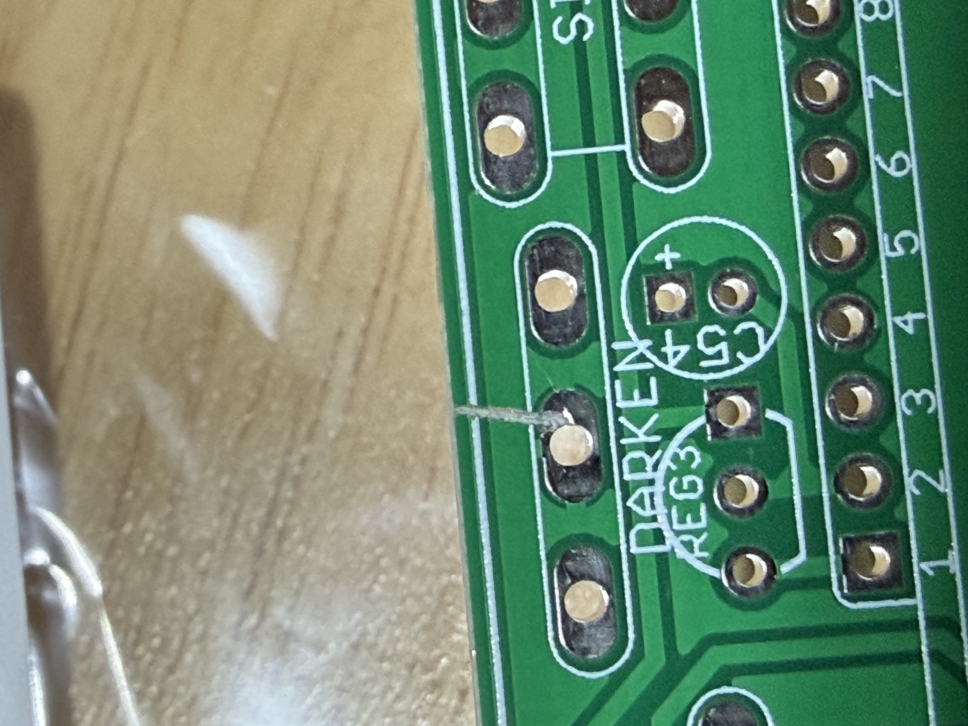
Hey all – I rec’d a Space Modulator PCB with a slight scratch in it running from the center leg of the Darken pot to the edge of the board. I took a pic (below) but went ahead with the build.
Fully built, I can’t get any power through the circuits (no f/x, no LED lighting, etc.). I’ve run a number of diagnostics, and can’t peg what’s wrong – I’ve gone as far as jumping the DC power direct from the D5 protection diode to Reg 3 (my understanding is that all regs share power), and I get full 9V power through the jumper wire, but it drops to 0V once I attach it to pin 1 of reg 3. I do still get 6.5 ohms running through to pin 1, however. D5 shows 8.6V coming out of the negative side so I should have some power flowing into the reg.
Anyone know if the cut in the PCB board could be the culprit, or is there something I’m missing?
TIA and cheers!
July 15, 2026 at 11:43 pm #39447BarryKeymasterThe white line at the top is just a decorative silkscreen border. I cannot say if you may have created a ground island though just below that (honestly I doubt it since the center pad has connections on either side of the scratch). I can’t tell how bad it is from your photo but you will be able to see that much better in person.
I would do a full re-flow as a cold solder joint is the number one offender in most forum posts.
Here is a complete build with gut shot to check against yours which can sometimes be helpful.
July 16, 2026 at 12:09 am #39448SoozayParticipantHey, Barry – thx for the response. The line I’m referring to is the vertical line that cuts through the silkscreen borders (and into the PCB surface itself). I’m wondering if it’s a trace cut that’s severed power to the components.
I’ve gone back and rechecked all key components for cold solders, bridges, etc.
Cheers!
July 16, 2026 at 12:49 am #39449BillyModeratorPost an image of the populated pcb it’s very easy to miss something even after multiple checks
The scratch as said doesn’t look too deep and that part of the circuit just looks like a low pass shelving filter to dump higher frequencies to ground
Lug 2 as you can see connects to ground and looking at the pcb image there’s no traces above the pot the 9v rail runs below it
July 16, 2026 at 12:12 pm #39450BarryKeymasterYes, I understand what you are referring to. My point was only that the scratch is very unlikely to be the source of the problem. As Billy pointed out, the power trace runs underneath that area, so it is not affected by the scratch.
July 16, 2026 at 1:26 pm #39451SoozayParticipantThanks for the confirmation, Barry. I won’t mess with it if it’s benign.
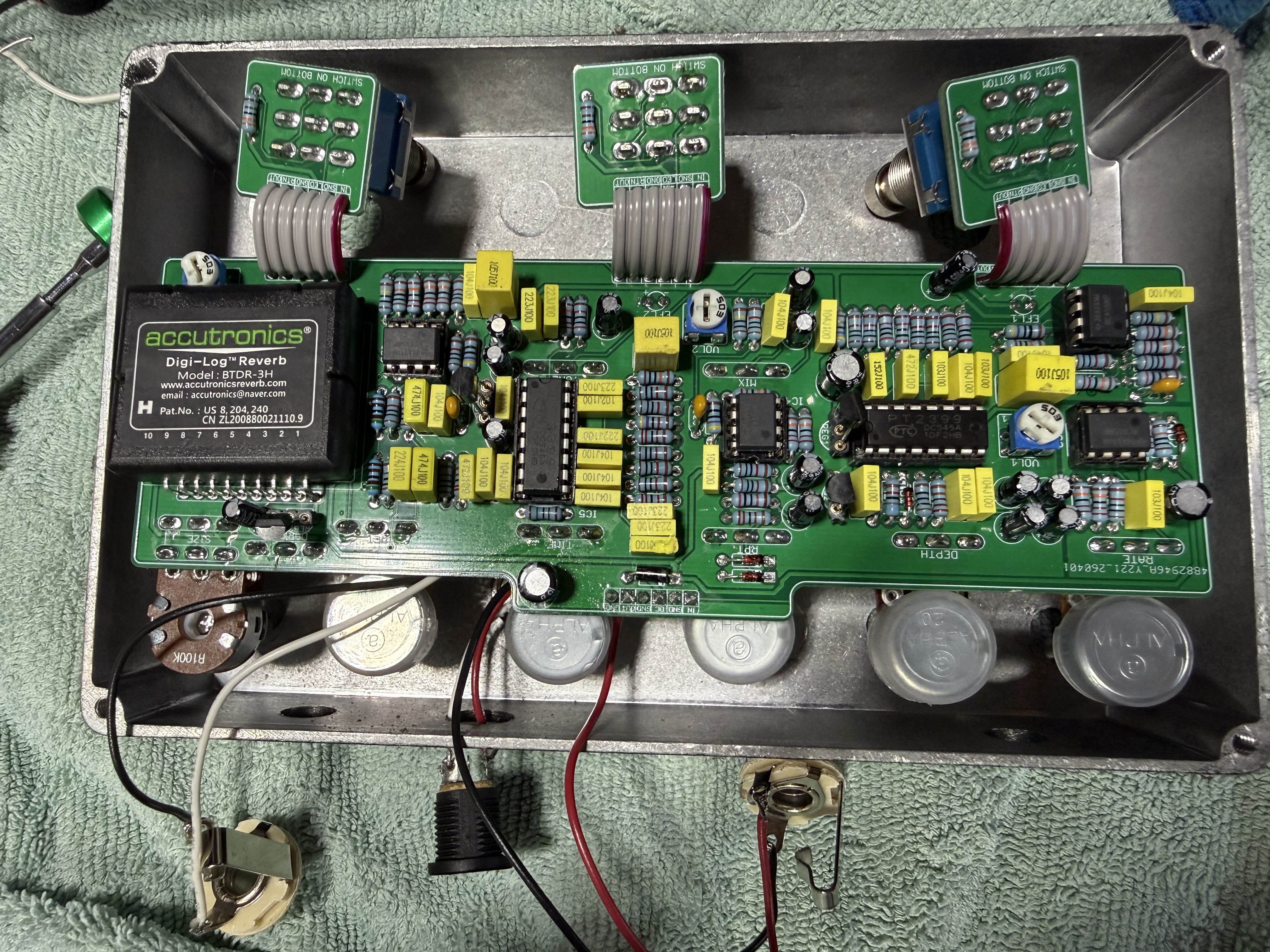
Here’s a pic of the full board:
July 16, 2026 at 2:08 pm #39452BarryKeymasterAt a glance I cannot make out IC6 well enough to confirm the correct orientation.
The other thing I would check is that all voltage regulators are firmly seated since sockets can create intermittent contact. You can make a few minor back and forth bends in the leads to assure they are secure in the sockets. Also tell us what brand of L78L05 that you used for all three.
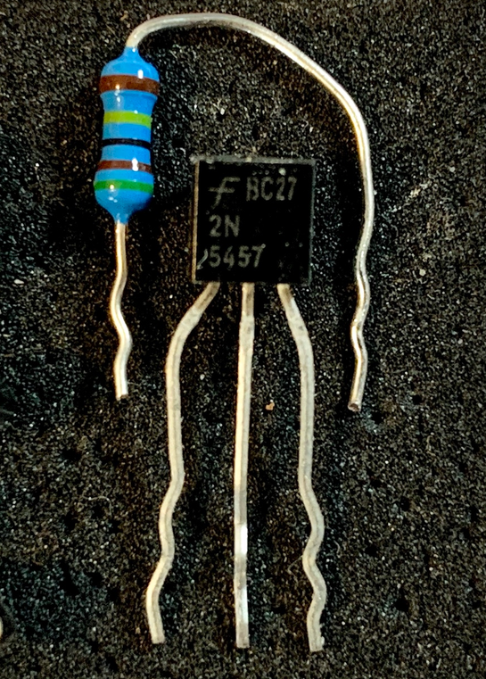
I would also set all three volume trimmers to their center positions.
Hopefully Billy can spot something.
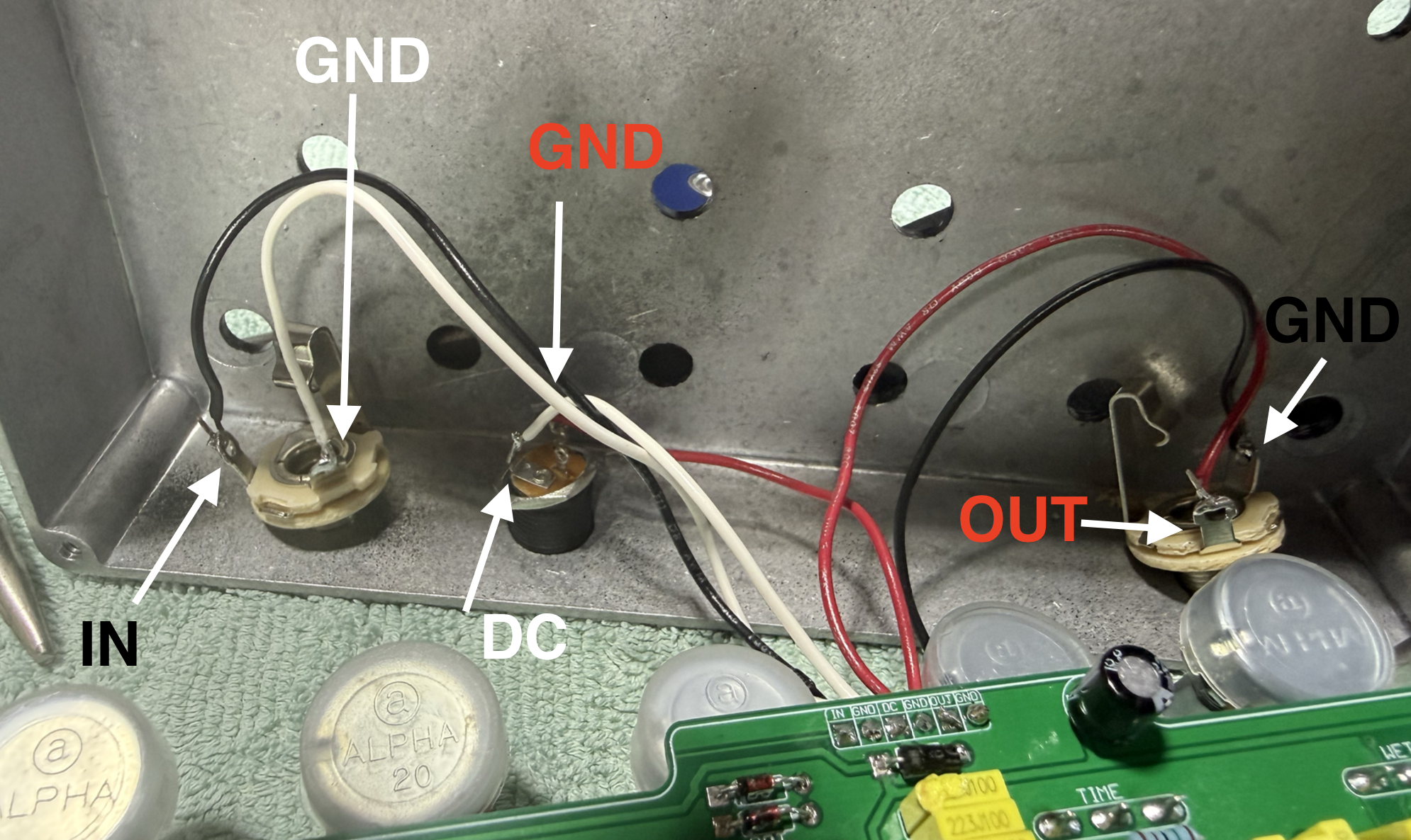
July 16, 2026 at 5:40 pm #39454brdModeratorWire color doesn’t matter, but I noticed it looks like you have a white wire going to the ground of one jack and a black wire going to the ground of the other. Can’t see where they go under the board. Maybe a shot of the other side of the board might help too.
July 16, 2026 at 8:04 pm #39455SoozayParticipantHere’s a diagram of the DC, input jack, and output jack. I’m pretty new at all this and I (admittedly) did a poor job of matching the wire colors to the right use. Font color = wire color. Really appreciate all of your help!
July 16, 2026 at 8:57 pm #39456BarryKeymasterAlso I was going to say that you need to make sure you have a power supply providing at least 100mA of current or it won’t work.
July 17, 2026 at 10:44 pm #39458SoozayParticipantThanks, Barry re: the 9V wiring. I’ve ensured that it’s in line with your diagram, and am using a 500 mA isolated power supply.
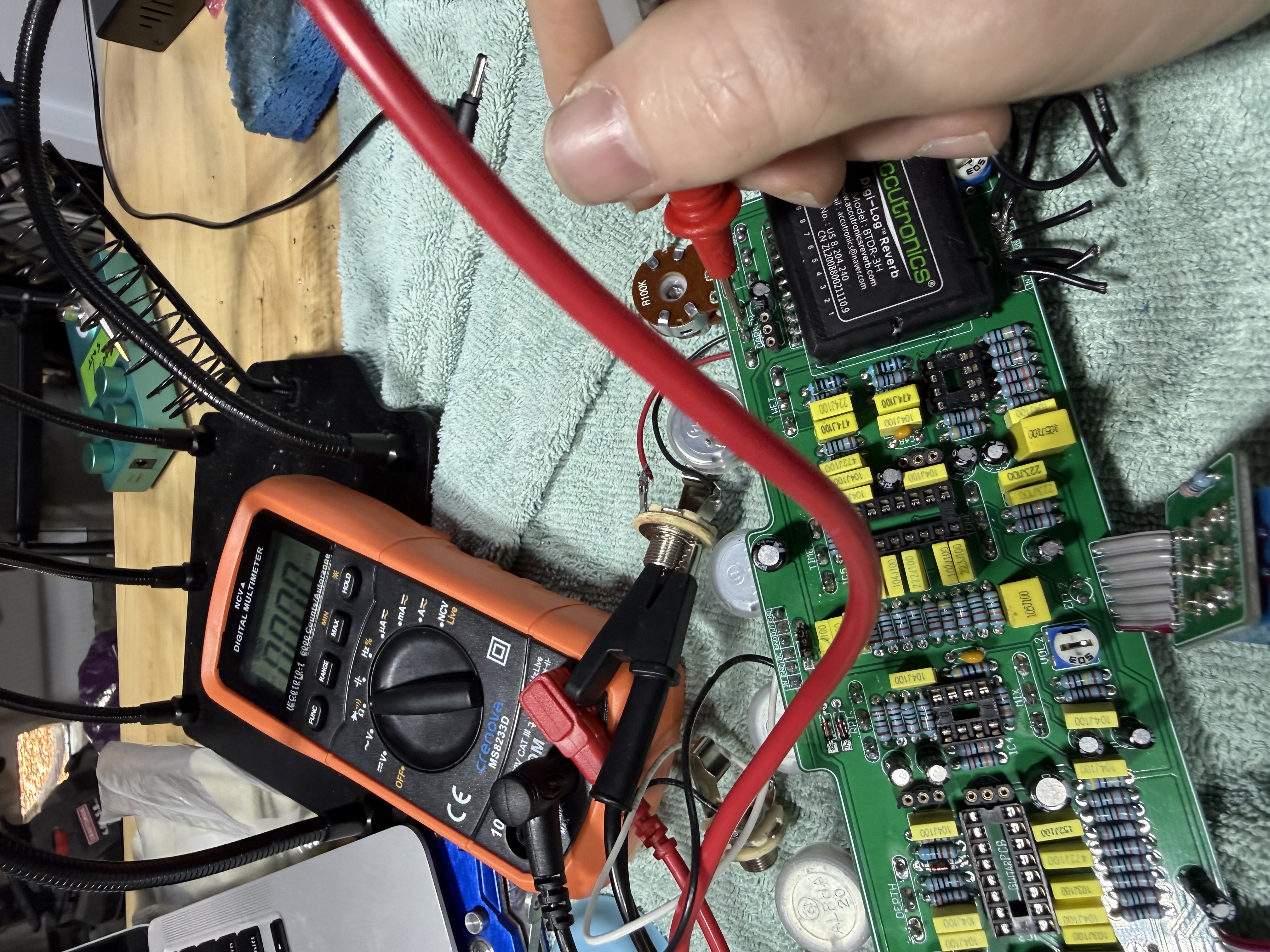
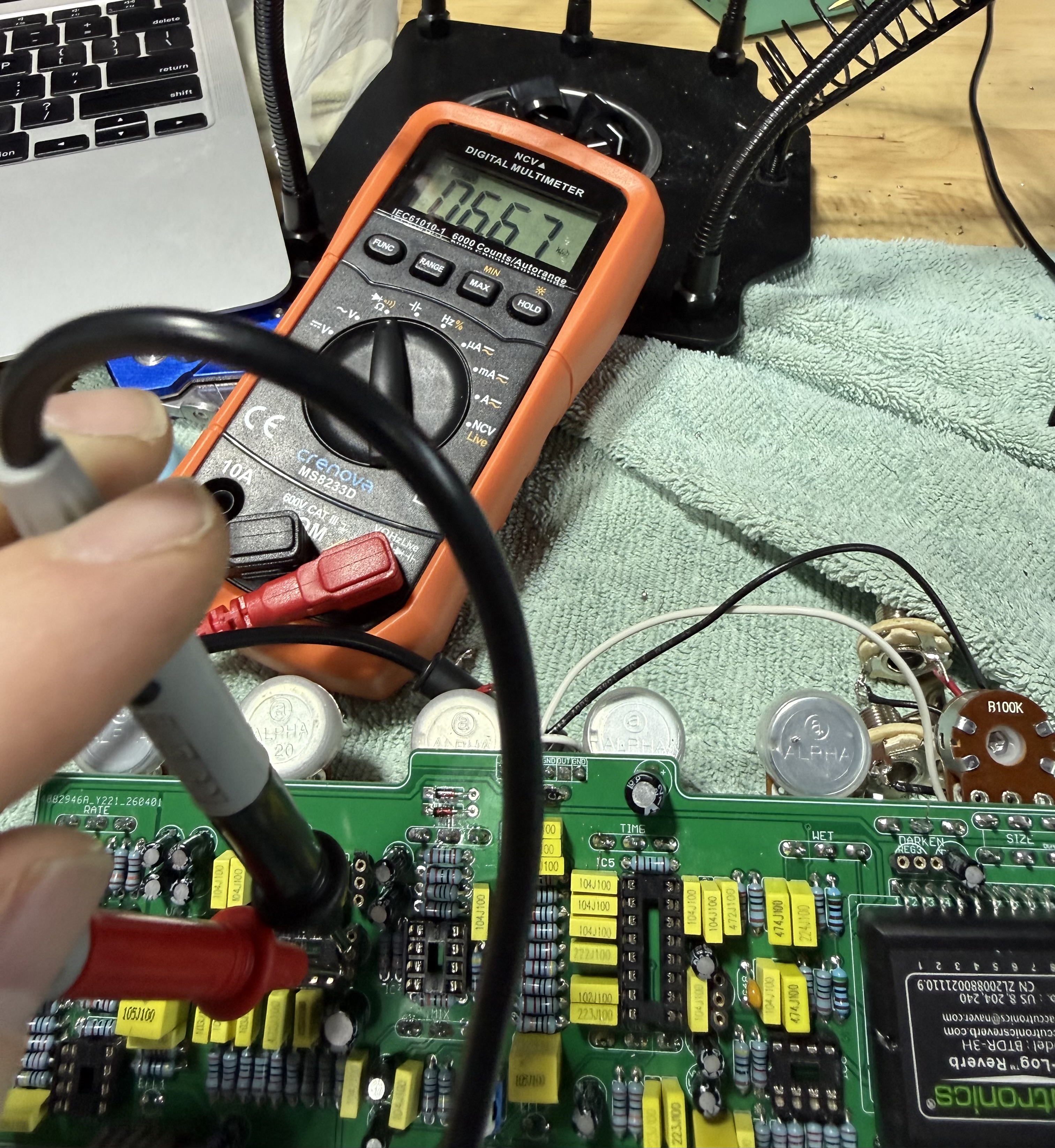
I’ve gone through and reflowed any suspect solder joints and have ensured there’s no solder bridges. I’m at a loss; I’ve taken out all of the transistors and chips and have performed some additional tests. The main 9V power rail is unshorted (measuring 6.6k Ohms at the empty regulator sockets), which should rule out any component assembly errors. However, there is a dead short of 0.0 Ohms between the middle pin of the Darken pot and the ground plane. (I’ve run a continuity test on the pot to ensure it’s in good shape.)
Pics of the readings:
July 18, 2026 at 8:31 am #39459brdModeratorIf you look at the schematic for the Reverb in the build doc, the center lug for the Darken pot goes to ground. Your observation just confirms that is as expected.
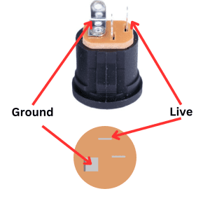
The previous picture of the power jack and wiring looked like you had the DC (white) and ground (red) on the wrong posts of the jack. Did you fix that? The large terminal is for the ground. (unless you are using a non standard power supply)
Problems if power jack wired backwards:
D5 is your reverse polarity protection, it should hold up to 9V reversed (briefly) but damage is possible. you should avoid bypassing that or subjecting it to prolonged reverse current. It could fail as an open or short.
Other circuit damage could occur if that diode fails or reverse current is applied to the rest of the circuit. i.e. LED damage.
I hope that helps
July 18, 2026 at 9:19 am #39460brdModeratorSorry, I couldn’t edit my previous post. I want to add that, if the power jack wiring was not the problem, an audio probe might be the best next step.
July 18, 2026 at 11:06 am #39461SoozayParticipantThanks, Barry. You’re right; appreciate your patience with me.
Regarding D5, I’m thinking now that if I had been multimeter testing the board with live voltage, I would’ve bypassed D5 completely and fried a component or two. Totally on me…
I’ll close this one out and ask the manufacturer if there’s a spare part or two I can buy to fix it v. starting from scratch.
Cheers, and thanks for your help!
July 18, 2026 at 11:38 am #39462brdModeratorDon’t give up on it. You put a lot of work into that build. When the power jack wiring is confirmed, be sure you have voltage through D5 then try each section of the build with a guitar. If one or more of the effects still isn’t working report back. If your LED’s work it’s a good sign.
An audio probe is still highly recommended.
I’m not Barry, but I did stay at a Holiday Inn Express last night (bad American humor)
July 18, 2026 at 11:44 am #39463SoozayParticipantHa! Apologies on the misidentification, brd! Still have sleep in my eyes (PDT)…
I”m not getting any LED lighting or sound.
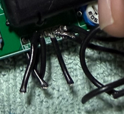
July 18, 2026 at 1:07 pm #39465BarryKeymasterIn the meantime I would take some time and carefully clean up the bottom 6-pin connector pads on the reverb side of the board.
I’d use a good Soldapullt-style solder sucker first, then follow up with some copper desoldering braid to remove as much solder from the holes as possible. Just be careful not to apply too much heat or linger too long, as you don’t want to lift or damage the pads.
Once the holes are cleaned out, I’d use individual wires instead of another ribbon cable. Insert each wire from the component side until the PVC insulation is flush against the board, then solder it from the opposite side and trim the excess just like you would a component lead. This helps prevent stray wire strands that could cause a short. Even if the holes aren’t completely cleared, individual wires are much easier to install one at a time than trying to force a new ribbon cable through.
Also if you bend Reverb brick leads to gain easier access be sure to reflow them all after bending it back.
It will not work with it like that above.
-
AuthorPosts




- You must be logged in to reply to this topic.