Your Source for DIY Pedal PCBs and NostalgiTone! › GuitarPCB Forum › GuitarPCB Build Support › Paramix Won’t Power Up
- This topic has 20 replies, 4 voices, and was last updated 2 years, 11 months ago by
 Cybercow.
-
AuthorPosts
-
June 3, 2023 at 10:11 pm #28828AnonymousGuest
Hey gang so this is literally my first purchase and build from pedalpcb…nice to be here.
so a couple things to keep in mind before I ask my questions, as you folks look at my build photos:
- I actually build stompboxes to mount horizontally in rack enclosures, with the knobs out front…so that’s why you’ll see all the pots/LEDs/switches on ribbon cable and removable headers.
- I switch between my rackmounted pedals with a loop switcher, so I always wire my pedaks up to be “always on”…so there are no 3PDT footswitches to be found in my builds.
OKAY SO ANYWAYS…
I’ve got the PCB populated with all the caps and resistors plus the TL074, done all the jumpers and component ommissions to build the most basic version of this circuit. I’ve added in the pots, the phase switch, and the bicolor LED. Also put in some power pigtails for testing. I have NOT wired in the input/output/send/return jacks yet.
So I then gator clipped on some 9V leads, and expected to see the LED come on red…NOTHING. Can you guys see any component mistakes or incorrect jumpering by looking at my photos?
Other question is, as-mentioned earlier I need to make this “always on” with no footswitch, and I’m wondering if someone can tell me the right way to jumper the S4/S5/S6 pads in order to make that happen?
THANKS and sorry for the long-ass post and weird build!
<p style=”padding-left: 40px;”></p>
June 4, 2023 at 1:01 am #28829CybercowParticipantIt looks like the two +9V pads have one red wire and one black (brown?) wire. If the red wire is the +9V and the black (brown?) wire is grounded – there’s the problem. And there is no ground wire connected to the GND pads. Where is the ground connected?
June 4, 2023 at 1:56 pm #28833AnonymousGuestYeah @Cybercow you are correct: it’s some 2-lead hookup wire from Amazon where the sleeve is silicon with both strands molded out of a single piece of silicon and then somehow in the manufacturing process they kinda “print” one side with black ink, which is a little janky and looks brown from a distance, ha-ha. You can see it much better in the mega-zoom photo I’ve attached.
You are also correct that I am attaching both the red (+) and black (gnd) leads to the two pads that are provided on the board and silkscreened with the label [+9V]
I guess I was assuming that the fact that there are TWO pads there implied that I was supposed to hook up both + and – to those two pads…not sure I understand why TWO +9V pads are provided if you are implying that’s the real deal?
So with that in mind I’m now assuming that I need to remove the “brown” lead and instead hook it up to one of the [GND] pads, yeah?
June 4, 2023 at 9:07 pm #28837CybercowParticipantCorrect. That PCB has two +9V connection points adjacent to one another. Often times, it’s helpful to have more than one +9V connection point. (I often use those 2nd +9V connection points to carry the PS over to other boards in combo builds.) Remove the wire you have going to ground from that pair and move it to one of the provided pair GND points next to the OUT solder points. Barry labels all of the solder points on his PCBs. It’s always good to pay close attention, avoiding such mistakes. 😉
June 5, 2023 at 9:42 am #28842AnonymousGuestNope. nuthin’. Still DOA.
June 5, 2023 at 8:19 pm #28845brdParticipantIf your definition of DOA is that the LED doesn’t light up. The S4/S5/S6 pads are connections that should go to the foot switch to activate the LED. Without a switch or jumper there the LED will not illuminate. If you want the LED to be on whenever the board is connected to power, a jumper between S4 and S5 should do the trick.
Hope that helps
June 6, 2023 at 8:46 am #28847CybercowParticipant“Nuthin'”? Did you try measuring the voltage across pins #4 & #11 on the TL074? It should be very close to the power supply.
And please, keep us updated with fresh pictures as you make these changes.
June 6, 2023 at 10:21 am #28848AnonymousGuestHey @brd so yeah I had actually asked that question about the proper jumpering for “always on” in my first post…
Other question is, as-mentioned earlier I need to make this “always on” with no footswitch, and I’m wondering if someone can tell me the right way to jumper the S4/S5/S6 pads in order to make that happen?
…and hadn’t gotten a response, so thank you for answering my other question.
Now that said, I have been keeping a little jumper around, and both before and after making @Cybercow ‘s suggested pad relocations, I had been “dry inserting” it in different combination pairs off of S4/S5/S6 to see if I got any kind of light-up on that LED, with no result. But now that you’ve given me a definitive answer on how to jumper that, I’ll solder it in properly and see if a really solidly-conducting contact makes any difference.
And I’ll take pics of all the new work as well, as-requested. Plus I’ll try @Cybercow ‘s voltage measurement suggestions to see if I’m getting power regardless of the LED as an indicator.
June 7, 2023 at 10:47 am #28851CybercowParticipantHow about R17? I notice it is NOT populated and it is one of the CLR resistors.
Also, are you using a common anode LED? A common cathode LED will NOT work.
June 8, 2023 at 10:37 am #28865AnonymousGuestHey, @Cybercow , regarding your question…
“How about R17? I notice it is NOT populated and it is one of the CLR resistors”
I shall quoteth from the build doc…
The Kill Switch turns off the effects loop (Send/Receive Loop). If you do not wish to install the Kill Switch, place a jumper between the pads of SW2A, omit D2 and R17, and ignore the wiring for SW2B.”
…so correct me if I’m wrong, but I was of the understanding that since I chose not to install the kill switch, and have done the most very basic version of that build, I should not have to populate that?
And then regarding your other question…
“Also, are you using a common anode LED? A common cathode LED will NOT work.”
…that may be a VERY good question that I had not thought of? To be honest, I had a bunch of red/green bicolor LEDs in my parts kit that were left over from a Muzzle Gate clone, and I just grabbed one, thinking “they were all the same”. I shall have to go back and look at my Tayda purchase order for those and figure out if I’m flat-out using the wrong kind!
I also still have not traced leads and looked for voltage on the TL074 as you had suggested, nor have I wired in the input/output jacks yet. SO heck really for all I know this think could already be working perfectly except for an LED that is not coming on…I’e just been too damned busy to investigate any of this over the last few days.
Thanks for your persistent interest and helpfulness, and I will for sure report back after I do all of the above!
June 13, 2023 at 6:18 pm #28930AnonymousGuestOkay so @Cybercow and @brd time to report in with my next phase of troubleshooting on this thing.
Good stuff first: the LED works splendidly now, due to me discovery that @Cybercow was correct about me using a common CATHODE LED…once I bought and installed a common ANODE LED—as well as permanently soldering in the jumper on S4/5 as @brd had mentioned…all good.
Slightly janky stuff second: voltage DOES in fact measure a solid 9V on pin four of the TL074 now, but the voltage on pin eleven is only running around 4V. Not sure if that tells you guys anything. Also P.S. I can’t imagine it’s possible I got this wrong because it’s the same no matter what direction you count from, but as a major newb, I want you guys to just take a look at the pins I circled on the photo of the PCB’s backside below this paragraph, and let me know if what I am “calling” pins four and eleven are ACTUALLY exactly that…?…
Bad stuff third: I’ve got the in/out/send/return lines hooked up now and it’s not passing any audio…I suspect I know why, but I’m gonna ask it here first before I desolder anything. If you guys could take a look at my second photo of the PCB’s front side below, and see where I’ve sketched in all the (+) and (-) leads for in/out/send/return…?…
So I have a feeling that this once again (like what I did earlier with the power leads) is where you’re going to tell me that Barry designed those so that the other pad in each of those four clusters is actually a second-and-identical positive connection point for each of those jacks, and that rather than soldering my ground wires into those points, I was instead supposed to connect my grounds for each of them to one of the available pads that is clearly-marked “gnd”? Am I right? Is that the issue? or did I actually solder into those areas properly, and this now is something else?
Let me know how I’m doin’…
June 13, 2023 at 8:44 pm #28931brdParticipantIn regards to pin identification, short answers is yes, I think you have the pins numbered correctly in the picture. However flipping the board over requires too much extra thought for me, I use the legs of the IC for checking voltages. From the top of the board, number 1 is the pin to the left of the little indent on then count down then over and up the other side.
As far as the wiring for the jacks, there is a “T” printed on the board to identify the pad that is connected to the Tip on the jack.
Now as far as the signal. You should check for output from both the send and the out jack. remembering the gain and mix pots should only affect the signal at the out jack.
Best
June 14, 2023 at 1:54 pm #28935AnonymousGuestHey @brd…so regarding your statement…
“As far as the wiring for the jacks, there is a “T” printed on the board to identify the pad that is connected to the Tip on the jack.”
…yes indeed I saw those and wired them in exactly that way the first time out—with my (+) leads from the jacks going to the [T] pads—HOWEVER the BIGGER issue I was trying to get across was: is the OTHER pad that is directly adjacent to the one marked [T] intended for GND? Or instead is it similar to how the power pads are set up, where I leave that second pad alone and do all my grounding elsewhere?
June 14, 2023 at 2:43 pm #28937BarryKeymasteris the OTHER pad that is directly adjacent to the one marked [T] intended for GND?
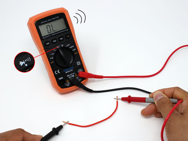
Yes, it is ground. You can test any pads by using your DMM in continuity mode.
Also, the reason for power sharing indicated by the group pads is for building combos in a single enclosure either in a pedal or a rack. For example, this rack contains all GuitarPCB circuits. Power sharing makes for easy, tidy, and secure wiring of not only the main circuit board but any mod boards, LEDs, Meters, or other add-ons located inside the same enclosure or Rack unit.
To find out more about combo builds, and power sharing there are guides on the Guides Page.
June 14, 2023 at 2:57 pm #28938AnonymousGuestYeah @Barry the power sharing concept makes sense.
Cool toys…your photo gives me massive G.A.S.!
I’ll check continuity on the grounds (good tip). That said, I’m still getting no audio through this thing, in spite of the fact that I appear at this point to have wired everything properly. As the Grand Beastmaster of guitarpcb, I’d love it if you could take a quick look at the last pics I posted and see if anything stands out as obviously amiss.
June 14, 2023 at 3:04 pm #28939BarryKeymasterOne thing not apparent in the photos is what type of Send Return Jacks are you using.
They must be this type (note the Tip on this jack):
June 14, 2023 at 3:23 pm #28941AnonymousGuestAhhh that’s IT! I’m guessing. I misunderstood from your instructions that those were only necessary if one was to incorporate that second set of jacks for the “II” and “IO” thing.
So I need that “patch bay” type that interrupts the signal…understood. I’ll get some.
-
AuthorPosts
 </p>
</p>


- You must be logged in to reply to this topic.